I started building an IGBT inverter using H-bridge topology. 2 Pairs of FGH50N6S2 IGBTs with RURG5060 anti-parallel diodes across them and a beefy 1uF cap on each leg. Measurements hardly showed any ringing but maybe it’s not a bad idea to add some extra snubber caps with resistors in the future.
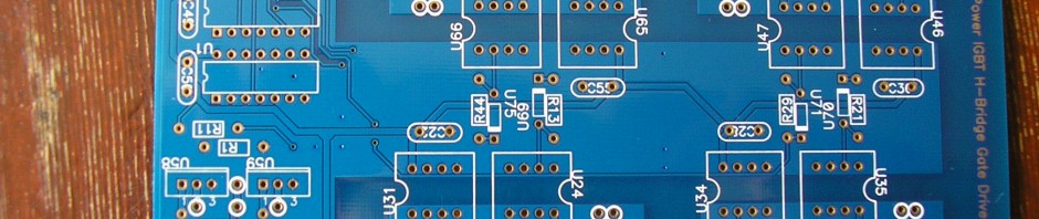
Here’s the very simple layout for the IGBT-board:

The IGBT driver board has 4 fully opto-isolated gate drivers. I chose to isolate all 4 drivers to get rid of any ground-noise that may arise from very high dI/dT (switching high currents really fast). It uses the MC33153Pcapable of sourcing 1 Amp and sinking 2 Amps to drive the IGBT gates. This is enough to switch on the IGBT in a little over 100nS and off in about 300nS. A simple digital opto-coupler (HCPL2601) is used to isolate the gate-drive signal from the rest of the circuit.
Schematic of a single gate driver (implemented on the driver board 4 times):
![P-CAD EDA - [Driver_AL]](http://www.nohup.nl/home/wp-content/uploads/2014/04/P-CAD-EDA-Driver_AL.jpg)
The 4 diodes in the top are just rectifiers for a floating alternating supply (no terminals shown).
Then there’s some basic logic to avoid illegal driving states (i.e. driving both gates turned on at the same leg causing shoot-through, turning the IGBT’s into small fireworks) and handle fault signals (IGBT Desaturation) from the MC33153P’s. Desaturation happens whenever the IGBT is unable to support the conducting current, due to which the Vce voltage gets dramatically high. A fault is detected when this voltage rises above 6 Volts, triggering a flipflop through an opto-coupler and blocks the drive-signals.
![P-CAD EDA - [Interface]](http://www.nohup.nl/home/wp-content/uploads/2014/04/P-CAD-EDA-Interface.jpg)
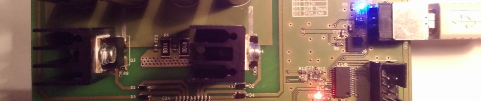
Last but not least, a floating supply for each driver. This is simply done by an SG3525A regulating pulse width modulator. It’s set to oscillate at a duty cycle a little under 50% at around 100KHz, driving a pair of IRFZ48Nmosfets, which in turn drive 3 toroidal transformers supplying the floating power to the driver circuits. I’ve only used 3 transformers since the supplies for the bottom IGBT drivers are wound around the same core: there’s no high dV/dT there, just some noise. I might even get away with powering both lower drivers from the same supply but this topology adds a little robustness to the system.
![P-CAD EDA - [PSU]](http://www.nohup.nl/home/wp-content/uploads/2014/04/P-CAD-EDA-PSU.jpg)
Finally a picture of the whole assembly. You can see the 3 transformers on the left and a little piece of prototyping board with a microcontroller (CY8C29466-24PXI) generating a pulse width modulated sine-wave for the driver board.

For more pictures check out the gallery
